Universal testing machine qualifies electronic components
Standardized shear force testing
Modern electronic products must meet a variety of characteristics. They are expected to perform better than their predecessor generations, but they should also be lighter, smaller or more robust. They must be able to withstand environmental influences such as temperature or humidity, and should endure mechanical stresses such as vibration or mechanical shocks – all this combined with an environmentally friendly manufacturing process and lower production costs.
A decisive factor for the reliability of an electronic product is the solder joint [1]. When it fails, the electronic product also fails [2].
Shear force test as classical testing method
Various tests are available to investigate the reliability of solder joints. As a conventional destructive testing method, the shear force test has become well established [3]. Changes in the solder joint that can, for instance, occur due to thermo-mechanical stress can be identified this way. The shear force is the measured quantity, which decreases with increasing degradation of the solder joint [3].
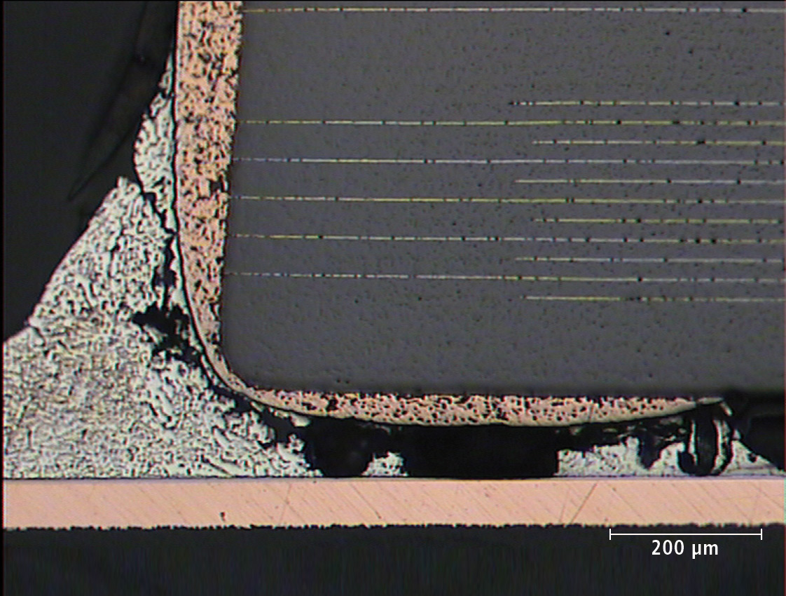 Figure 1: Crack formation at a solder joint due to thermo-mechanical stress (transverse metallographic section)
The tests are normally carried out with a small set of different materials prior to the start of production within the scope of product qualification. As a rule, these include various solder pastes that are necessary for the connection between substrate and component and various printed circuit board metallizations. These tests must also be performed when the solder paste is changed, for instance during an ongoing production process. The shear forces can be determined on real components, for instance on circuit boards of a mobile phone, or on a test assembly. Due to statistical fluctuations of individual component failure it is advantageous to carry out the tests with a sufficient number of identical components [3]. As these are usually not available in large numbers, a test assembly is to be preferred.
The underlying DIN EN 62137-1-2 norm states that the measuring device for carrying out the shear test merely must “include a mechanism for mounting the substrates …” and “can exert a shear force that is greater than the strength of the soldering connection …” The recommended feed rates in DIN EN 62137-1-2 are between 0.5 mm/ min and 9 mm/min.
Universal testing machine for shear tests
In addition to the specialized shear test devices available on the market it is, consequently, also possible to use a universal testing machine for carrying out shear tests. The Japanese norm JIS Z 3198-7 (2003) [5] explicitly allows the use of a universal testing machine. The speed range for testing specified in the Japanese JIS Z 3198-7 is between 5 mm/min and 30 mm/min. The implementation of the normative standards for carrying out shear tests using Shimadzu’s AG-X universal testing machine with the 90° shear test kit is described below.
A test board with M-MELF and 1206 type components were used as test objects applying a lead-free tin-silver-copper soldering paste and a chemical-gold circuit board metallization, as well as a test circuit board with SMD capacitors in sizes 2512, and also a chemical-gold circuit board metallization using a tin-silver-copper soldering alloy. The individual component types were each soldered in a row onto the circuit board. This leads to more economical testing procedures, as the circuit board does not need to be readjusted prior to each measurement.
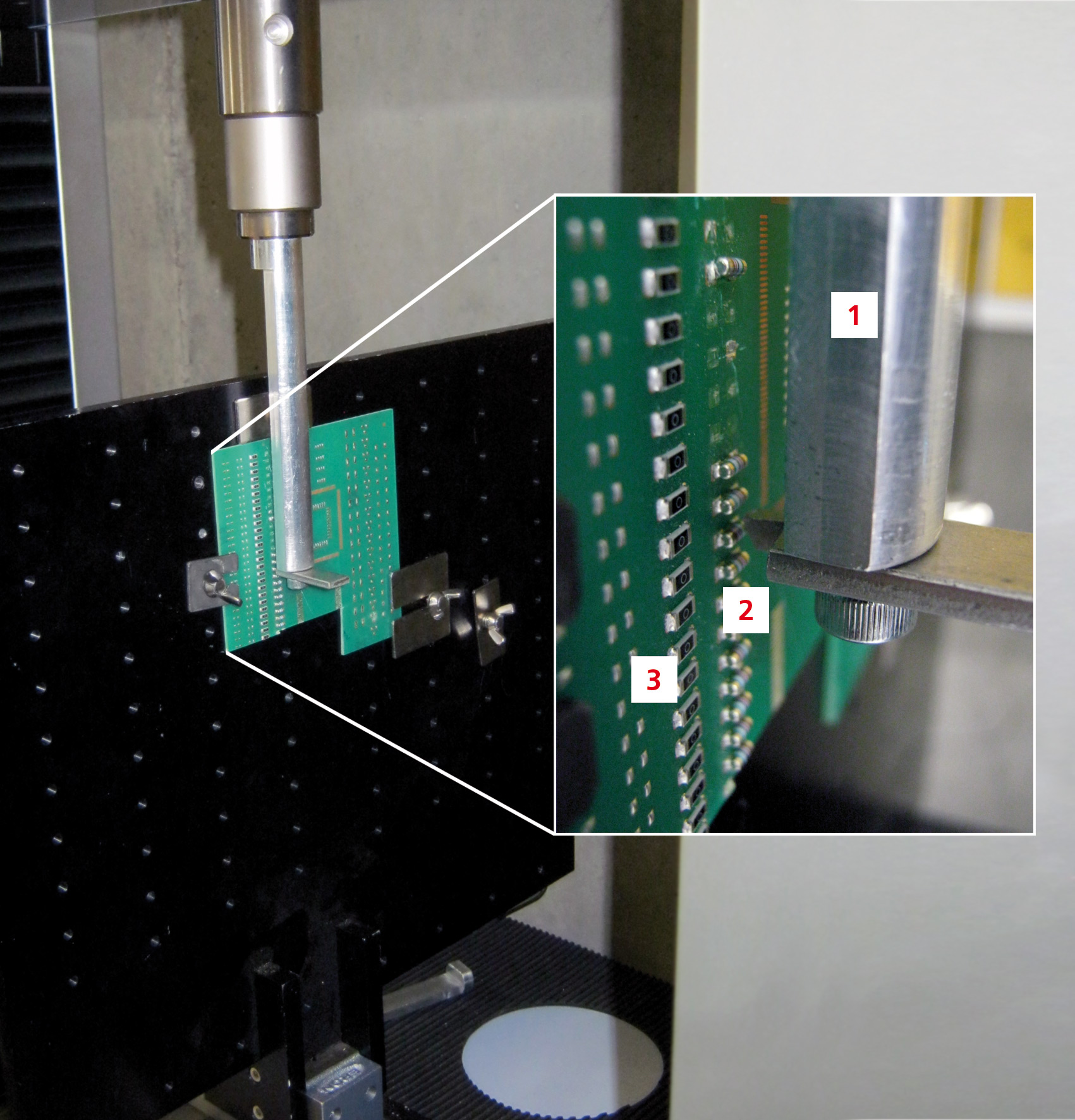 Figure 2: AG-X shear test assembly with (1) = shearing chisel and (2) = M MELF type components (3) = 1206 type components
Implementing the shear tests
The circuit board is mounted on the breadboard of the shear test kit with slotted clamping plates and positioned via micrometer screws (Figure 2). It has been proven advantageous to drive the shearing chisel up to the point where it contacts the circuit board. This point can be easily recognized on the micrometer screws, as these will no longer indicate any distinct change in length.
Subsequently, the shearing chisel is adjusted to the desired component distance h via the micrometer screws (see figure 3). A value of 0.1 mm has been found suitable. According to DIN 62137 the shearing height, which is the distance of the circuit board to the shearing chisel, should not be greater than ¼ of the component height. During the shear test, one has to make sure that the shearing chisel does not rub against the solder pad of the circuit board or against the solder deposit.
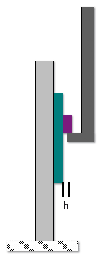 Figure 3: Schematic of the shear test geometry.
A stainless steel chisel was custom-made for each component width, which can be screwed onto the standard mount of the shear test kit of the tensile strength testing machine, was used as shearing chisel. The shear rate was set to 5 mm/min and automatic recognition of the sample fracture was activated in the measuring method.
After the start of the measurement and the automatic sample fracture recognition, the sheared component is removed from the shearing chisel using tweezers. The shearing chisel is subsequently moved up to the next component via manual control of the tensile strength testing machine and a further measurement is started.
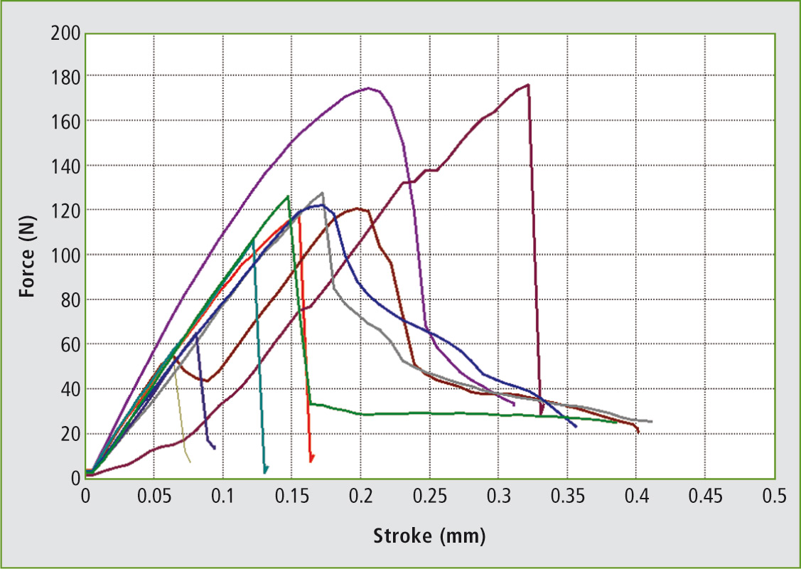 Figure 4: Example of a shear force diagram for ten components of size 2512
For evaluation, the maximum strength is primarily of interest. In case of questionable fracture patterns during optical inspection, the force-displacement diagram is used to detect possible non-uniform shearing. This can occur when the shearing chisel has not sheared off the component horizontally, but due to displacement of the component only one side of the component has initially been sheared off. Such shear patterns can be clearly recognized in the force-displacement diagram. Via the overlay function of the Trapezium-X software, it is possible to display several measuring curves superimposed in one diagram (Figure 4). This way, it is possible to evaluate the quality of several solder joints at a glance.
After shearing, the remaining residual solder joints are examined under a microscope and classified according to their fracture mode (Figure 5). In the current example fractures only occurred along the solder/component interface and diagonally across the solder (see figure 5, component a and component b).
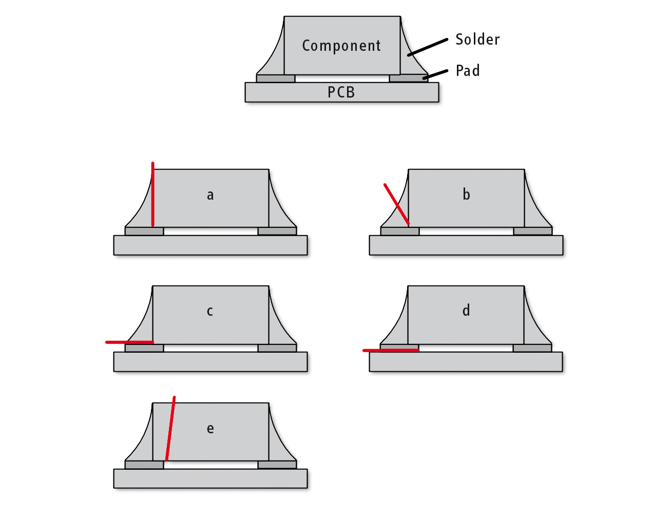 Figure 5: Fracture modes (modified according to [6])
Conclusion
After carrying out several hundred shear tests according to the method described, it can be concluded that shear tests can be performed according to the relevant standards using a universal testing machine. A comparison of the determined shear forces with the shear forces documented in the literature [6] shows a similar dispersion of the measurement results.
To determine the influence of soldering defects, such as porosities on the shear forces and their dispersion, it is possible to first examine the samples using a non-destructive method, for instance 2D X-ray testing or computer-assisted tomography and to classify them according to their proportion of porosities [7].
Due to the typical features of the universal testing machine, it is also possible to carry out cyclic tests on SMD components without shearing, using custom-made shearing chisels. The first of such tests carried out have been promising so far.
Acknowledgement
Aschaffenburg University of Applied Sciences thanks Shimadzu for its professional support and collaboration as well as for supporting our teaching and research activities.
Author
Prof. Dr. Michael Kaloudis
Aschaffenburg University of Applied Sciences, laboratories for materials technology and structural-design and connection technologies
References
[1] Shnawah DA, Sabri MFM, Badruddin IA (2012) A review on thermal cycling and drop impact reliability of SAC solder joint in portable electronic products. Microelectronics Reliability. Doi:10.1016/j.microrel.2011.07.093
[2] Suganuma K (2001) Advances in lead-free electronics soldering. Current Opinion in Solid State and Materials Science. Doi:10.1016/S1359-0286(00)00036-X
[3] Dusek M (2002) Test methods for evaluating the reliability of PCB finishes using lead-free alloys: A guide. MATC A 107. National Physical Laboratory, Teddington
[4] DIN Deutsches Institut für Normung e.V. Oberflächenmontage-Technik – Verfahren zur Überprüfung von Umwelteinflüssen und zur Prüfung der Haltbarkeit von Oberflächen-Lötverbindungen Teil 1-2: Scherfestigkeitsprüfungen. Beuth Verlag (DIN EN 62137-2)
[5] Test methods for lead-free solders. JIS Z 3198-1 2003. Japanese Standards Association, Tokyo, Japan
[6] Ahrens T, Andreae H, Schruttke W (2006) RoHS-Handbuch für Hersteller und Zulieferer: Praktische Umsetzungshilfen, alternative Materialien und innovative Verfahren. Forum Verlag Herkert, Merching
[7] Rauer M, Volkert A, Schreck T, Härter S, Kaloudis M (2014) Computed Tomography-Based Analysis of Voids in SnBi57Ag1 Solder Joints and Their Influence on the Reliability. J Fail. Anal. and Preven. Doi:10.1007/s11668-014-9801-y