Shining a light on clean energy
The UV-3600i Plus as a research tool for organic photovoltaic materials
Frederik Kiel, Prof. Cemal Esen, Ruhr-University Bochum
Photovoltaics is an important pillar of the energy revolution and is more topical than ever before as a research field. Classic rigid silicon solar cells have long been part of everyday life – from pocket calculators to large solar modules in private homes and industrial solar parks. In the future, flexible or even transparent solar cells made from organic materials could enable an even wider range of applications. The development of high-performance UV-Vis spectrometers is valuable for identifying and testing materials or cell prototypes and paves the way to technically sophisticated products.
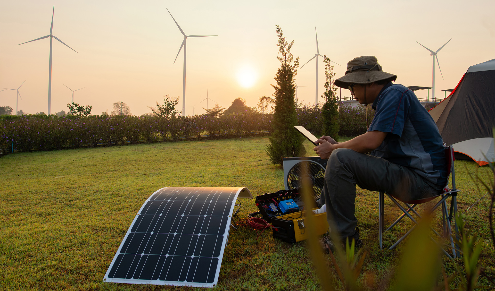

The current and future challenges facing humankind in terms of climate protection and energy supply require a broad approach to energy conversion, storage and recovery. Photovoltaics is already an integral part of the current energy mix, and this will steadily increase in the future. The continued development of organic photovoltaics (OPV) and its production processes also plays an important role here. The aim is to have flexible solar cells that can be manufactured locally and can reduce dependence on fossil fuels.
OPV cells can be wet-chemically applied to flexible substrates such as polyethylene terephthalate (PET). The resulting dry layers have layer thicknesses in the
Basic research in “EffiLayers” project
In its “EffiLayers” project, the Chair of Applied Laser Technologies (LAT) at Ruhr-University Bochum is working with the partners Coatema Coating Machinery GmbH, LIMO Lissotschenko Mikrooptik GmbH, Ortmann Digitaltechnik GmbH and Fraunhofer Institute for Laser Technology on the process optimization of the roll-to-roll (R2R) production of innovative, highly efficient organic photovoltaic cells. This involves the selection of materials and laboratory-scale evaluation for the subsequent R2R process, the evaluation of processes for improved processability (e.g. surface treatment) and the substitution of conventional process technologies with photonic technologies (e.g. laser drying).
For each of these tasks, the acquisition of the transmission/absorption spectra using the UV-3600i Plus is an essential part of the subsequent evaluation. In addition, the spectra make it possible to evaluate numerous parameter variations in a single layer in advance without the laborious process of manufacturing complete cells.
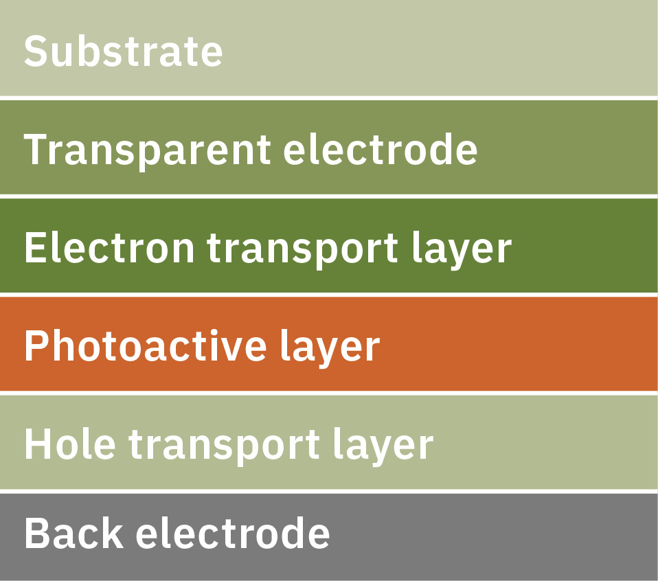
Checking the electron transport layer including anti-reflective function
Starting with a transparent substrate (PET) with a coated, transparent indium tin oxide (ITO) electrode, the first layer to be applied is the electron transport layer (ETL). By adjusting the energy levels, negative charge carriers can be transported, while positive charge carriers are blocked to avoid recombination. Just like the substrate and the transparent electrode, this layer should have a high transmission rate so that as many photons as possible can reach the photoactive layer for generating charge carriers. In OPV, zinc oxide (ZnO) is a commonly used material for wet-chemical coating.
Figure 3 shows the transmission spectra of the base substrate PET/ ITO and ZnO layers of dispersions from different providers applied to this, measured with a Shimadzu UV-3600i Plus with an ISR-603 integrating sphere. The absorption spectrum of the photoactive poly (3-hexylthiophene-2,5-diyl) layer with phenyl-C61-butyric acid methyl ester (P3HT:PCBM) is also plotted to illustrate the spectral range relevant for charge carrier production. The transmission here is over 80% for the base substrate. The application of the ETL layer improves transmission regardless of the provider.
Further investigations with the integrating sphere show that this is due to a reduction in reflection by the electron transport layer (Figure 4). Zinc oxide has a lower refractive index than indium tin oxide and thus forms an anti-reflective layer. However, this refractive index varies greatly, especially in the case of wet-chemically produced thin films, due to factors such as solvent, particle size, post-treatment and the resulting homogeneity and crystallization of the dry layer. With a refractive index of n1 = 1.63 for ZnO[1], the optimum layer thickness d of a ZnO anti-reflective coating at 515 nm is as follows:

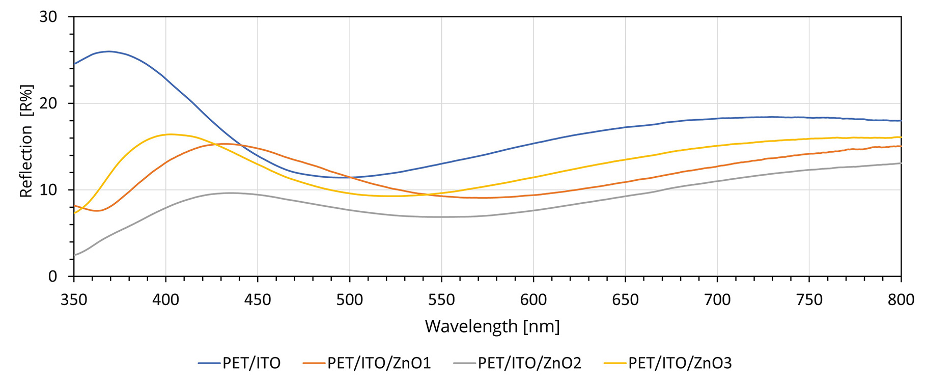
The targeted layer thickness of the electron transport layer is significantly lower (approx. 20 nm), due to the poor conductivity of the zinc oxide layer. While the materials “ZnO2” and “ZnO3” have better transmission properties, this is not reflected in the efficiency of the OPV cells produced using these materials. Compared to an OPV cell without ETL, the efficiency of these materials is 80% better. However, with the “ZnO1” layer, it is 120% better. This is primarily due to the smaller particle size distribution (5–10 nm) of “ZnO1” compared to “ZnO2” and “ZnO3” (20–30 nm), since the latter cannot achieve the desired layer thicknesses of the ETL.
Analysis of the impact of heat treatment
Another way to reduce production and system costs is to dry the wet-chemically applied layers via laser drying.[2] For the photoactive layer Poly(3-hexylthiophene-2,5-diyl):Phenyl-C61-butyric acid methyl ester (P3HT:PCBM) the heat treatment serves not only to dry the solvent but also to ensure crystallization of the P3HT. This results in a red shift in the absorption spectrum so that even lower-energy photons can be absorbed improving the efficiency of the OPV cell.
Figure 5 shows this shift in the main absorption peak from 485 nm without drying, 500 nm with the optimum laser drying parameter set and up to 515 nm with conventional heat treatment (heating plate, 2 min at 140 °C).
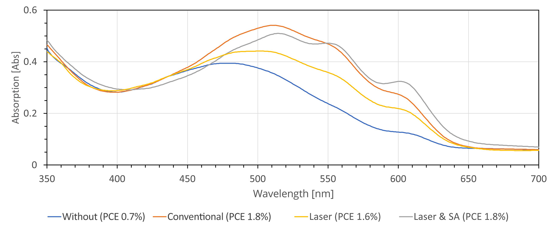
Measurements showed that laser drying improves crystallization and, based on efficiency measurements, also ensures sufficient drying, but it is not sufficient on its own to achieve optimum cell performance. However, the additional process step known as “solvent annealing” (SA) leads to a comparable spectrum of the layer and enables a similar level of cell efficiency to be obtained. In this process, the layer is exposed to a solvent-containing atmosphere for a short period of around 10 seconds, which facilitates crystallization because the molecules remain in a mobile phase for longer. The peaks at the longer wavelengths of 550 nm and 600 nm are even more pronounced.
Impact of surface treatment – surprising findings
A difficulty in coating the hole transport layer of poly (3,4-ethylene dioxythiophene) with polystyrene sulfonate (PEDOT:PSS) results from the relatively high contact angle of the PEDOT:PSS dispersion on the photoactive layer. Contact angles of less than 25° are required for effective wetting of the fluid on the substrate. Larger contact angles lead to inhomogeneous coating and even to completely uncoated areas (Figure 5). By diluting the dispersion with less polar solvents, the contact angle can be reduced to less than 30°. However, all coating parameters change due to the reduced solids concentration, while the drying effort is considerably increased as a result of the greater wet layer thickness.
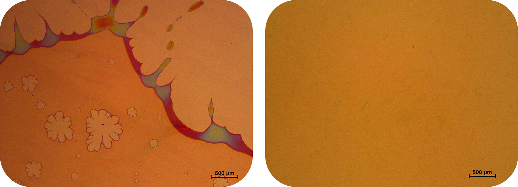
Another way to improve the contact angle is to increase the surface energy on the substrate. This can be achieved by means of irradiation with a UV excimer lamp. The photons of the lamp used are highly energetic (172 nm or 7.2 eV) and can break up the molecules of a variety of organic bonds or oxides.
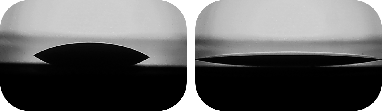
The high-energy radiation also generates ozone between the beam source and the sample. This results in an intensity drop of 80% at a distance of 6 mm. The efficacy of the irradiation is shown in Figure 7: On the untreated substrate, the droplet forms a contact angle of 26°; after excimer irradiation, it is well below 20° (minimum value due to measurement technology). Treatment efficacy depends on the radiation dose and therefore on the distance and duration of exposure. Even at distances of 25 mm, an improvement in the contact angle to less than 20° was demonstrated.
However, since the photoactive layer is also organic material, further investigations are needed to identify and evaluate any further effects of UV radiation on the material. Evaluation of the absorption spectra (Figure 7) reveals a decrease in absorption for all treated layers and a blue shift in the main absorption peak from 505 nm to 500 nm at a distance of 20 mm and to 495 nm at a distance of 10 mm.
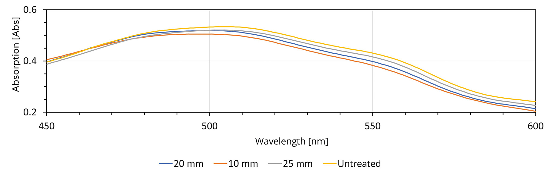
A comparison of the electrical parameters shows that although the wettability of the photoactive layer has been improved by UV radiation, it does not outweigh the deterioration of the optical properties. The efficiency of the cell prepared at a distance of 25 mm is already reduced by 25% compared to the untreated cell. This also applies to the short-circuit current which is related to the absorption height (level of absorption). The cell prepared at 10 mm demonstrates a 75% reduction in efficiency. In addition to a reduced short-circuit current of 50%, there is also a reduction in the open circuit voltage of 15%. This is also related to the wavelength of the main absorption peak.
Conclusion
In organic photovoltaics, spectroscopy plays a key role in comprehensive sample and material characterization. Thanks to this, it is often possible to evaluate the theoretical suitability of materials, individual layers or processes in advance without the need to construct entire cells. In addition, it provides information that enables a better understanding of cell performance based on a complex interaction of optical, electrical and interface-dominant properties.
Literature
- Stelling, C., Singh, C., Karg, M. et al., “Plasmonic nanomeshes: their ambivalent role as transparent electrodes in organic solar cells”, Sci Rep 7, 42530, 2017. https://doi.org/10.1038/srep42530
- F. Kiel, C. Esen, A. Ostendorf, und V. Wirth, „Solvent evaporation and annealing of solution-processed organic materials by laser irradiation on flexible substrates“, gehalten auf der Lasers in Manufacturing (LiM) 2021, 2021, Publiziert