Circuit board failure analysis
Infrared microscopy
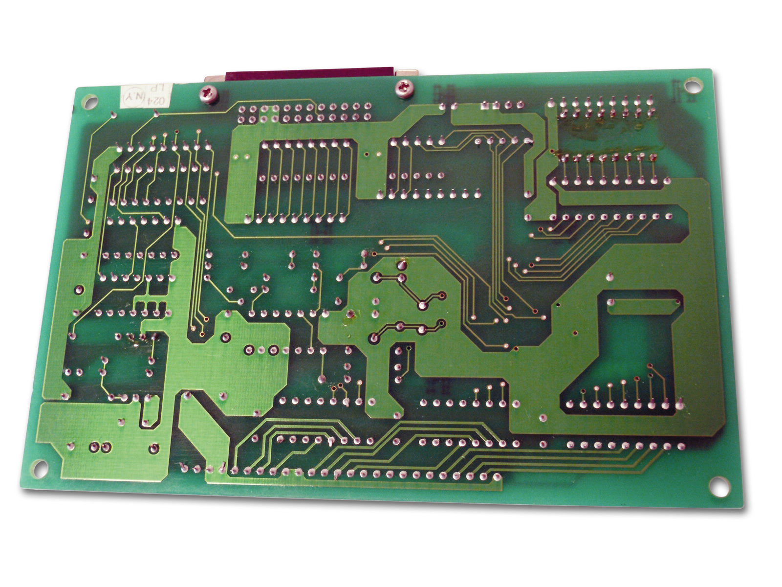 Figure 1: View of a typical circuit board with faultless circuit
Non-destructive materials testing can be carried out using ATR (‘Attenuated Total Reflection’) microscopy. ATR measurement is used to identify not only the material but also its physical condition. What causes imperfections such as caverns, bubbles or failures in circuit boards? The manufacturer or user of the board needs to know. How can these imperfections be identified? Infrared spectroscopy provides the answer.
For this case, the IRPrestige-21 FTIR spectrophotometer was used in combination with the AIM-8800 infrared microscope and the ATR-8800M objective.
The ATR objective is equipped with a Germanium crystal. The objective head is placed on the sample surface, an infrared beam is passed through the sample at a 30° angle and is reflected off the sample. The beam penetrates approximately 1 µm into the sample surface and records spectral information of the material. Contact surface diameter of the objective is about 50 µm.
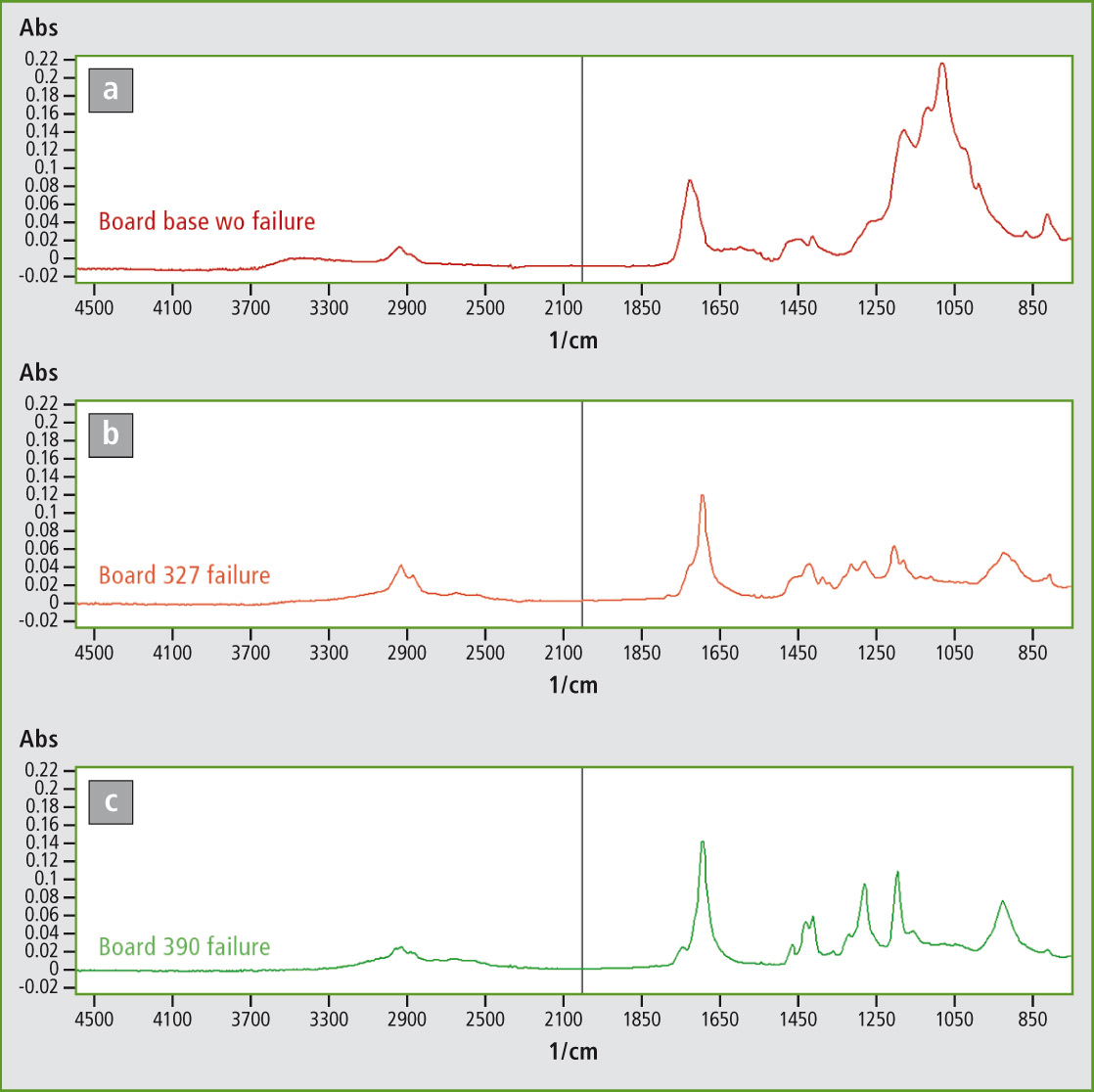 Figure 2: Three infrared spectra resulting from micro-ATR measurement of a circuit board: (a) dark-red line: spectrum of circuit board surface, (b) red line: spectrum of a failed surface, (c) green line: spectrum of another failure
In the diagram above, all three infrared spectra are superimposed and the section at 1700 cm-1 has been expanded. The different band positions of the CO signals can be clearly distinguished. The signal at 1720 cm-1 originates from the circuit board backing material and the signals at 1690 cm-1 arise from the failures.
Cause of failure identified
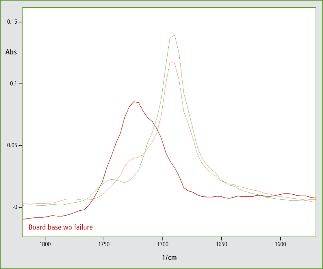 Figure 3: Section of the spectrum of figure 2, representation of the different band positions of the carbonyl groups
Boards are manufactured – de-pending on quality – from fiberglass mats in a network of resins or from paper impregnated with resins or phenols. The infrared spectrum (a) in figure 3 shows typical features of silicone (broad bands at 1200-950 cm-1) and resins (~ 1720 cm-1, -C=O, for instance acrylic resins band). In individual measurements for the determination of failures, additional spectra were detected. These can be observed in spectra (b) and (c). In all failure spectra, the dominant signal of an acid at 1690 cm-1 ([-C=O]-OH acidic group) is evident.
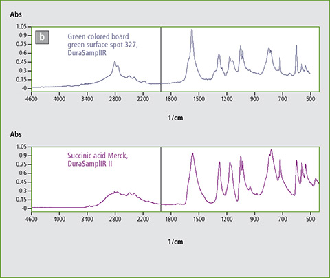 Figure 4: Spectral library search for spectrum (b) closely matches the spectrum of succinic acid
Spectrum (b) was derived from one failure and closely matches succinic acid (amber). Amber is a natural resin. Library search for spectrum (c) closely matches adipic acid.
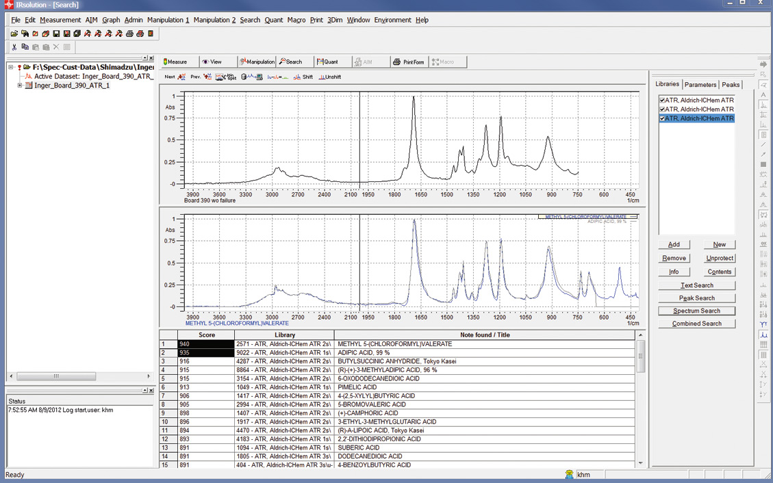 Figure 5: Spectrum (c) and search result of the Aldrich-Ichem library of STJapan-Europe. Adipic acid was a hit.
The range of failure
With this knowledge, larger areas can also be analyzed using the ‘mapping’ function. Figures 6 and 7 show a map of the failure on the circuit board.
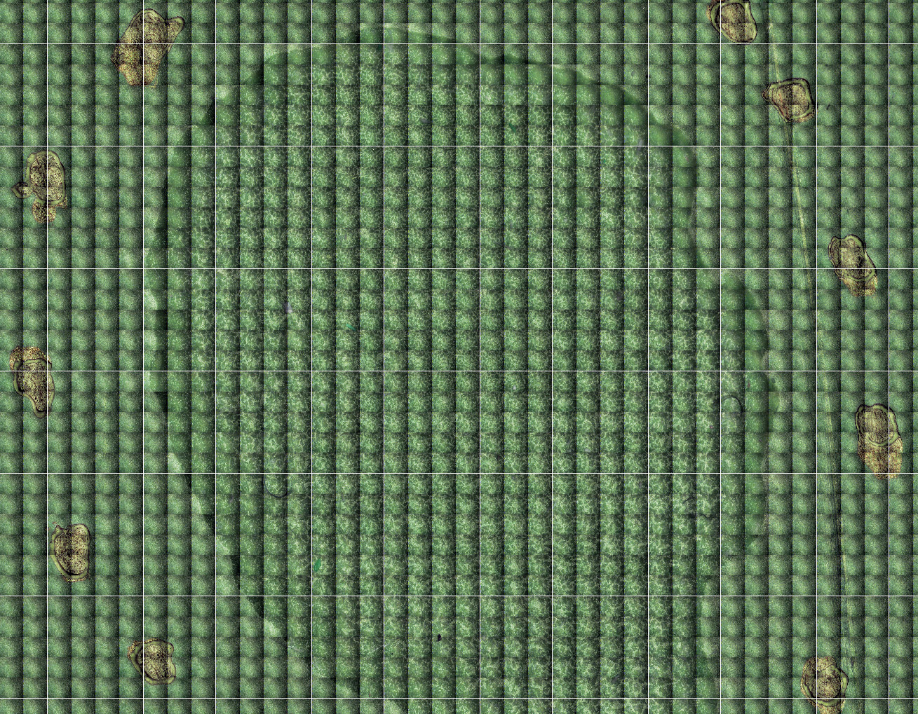 Figure 6: Representation of the mapping in observation mode on a selected visible area of the sample. The view was created from 400 x 300 µm frames.
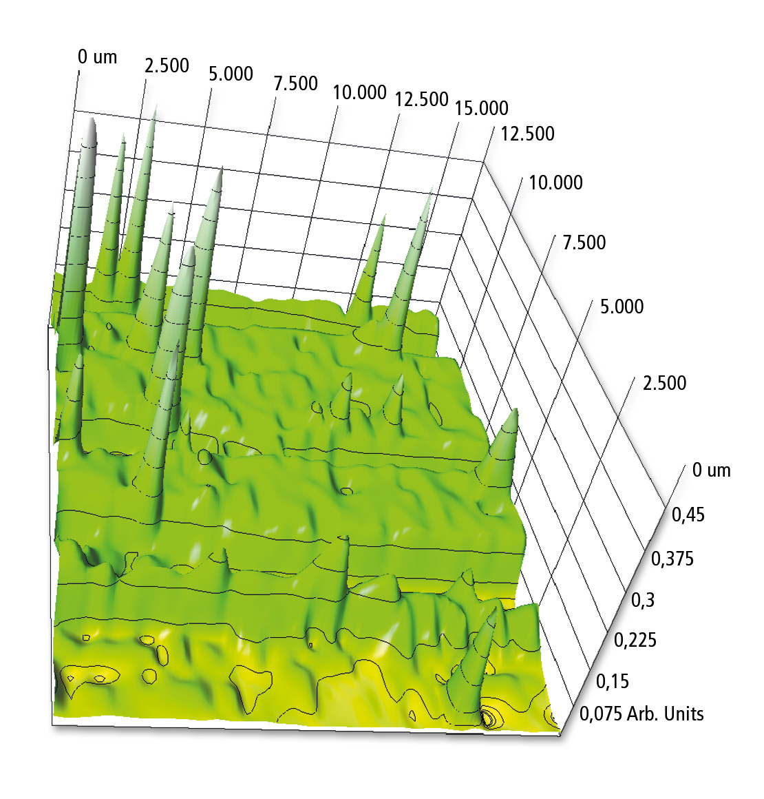 Figure 7: 3-D view of analysis of 800 infrared spectra, with area mapped against intensity at an analytical wavelength of approximately 1700 cm-1
The view in figure 6 of the circuit board was obtained from images as 400 x 300 µm frames. Measuring area corresponds to an area of 1.25 to 1.65 cm. 800 spectra were measured with an interval of 500 µm.
The 3-D map of the analysis of a circuit board is shown in figure 7, where area has been mapped against intensity of a selected wavelength. The maxima in the figure point to changes on the surface. All the maxima correspond to the spectrum of the coating with a signal of the CO bands at 1690 cm-1. Spectrum (a) of the backing material from figure 1 is found in the flat areas. This view is indicative of an unevenly distributed layer and various layer thicknesses. Where only spectrum (c) was found, the layer thickness was at least 1 µm, while the other positions represent layer thicknesses of less than 1 µm.