Hungry water:
Ultrapure water monitoring in the nanometer fab
Markus Janssen, Shimadzu Europa GmbH
How a process engineer and a new online TOC analyzer keep microscopic defects off semiconductor wafers
In a modern semiconductor fab, yield – the percentage of working chips produced on a single silicon wafer – decides whether a new process is profitable. Yet even in spotless cleanrooms, invisible contaminants in the rinse water can undermine months of optimization. This story follows process engineer Lena as she traces an unexpected rise in wafer defects back to the “hungry water” that washes every layer, and how online total organic carbon monitoring helps her see what the water has been hiding.
Red alert: A silicon wafer map exposes a threat
On a night shift in a modern semiconductor fabrication plant, or fab, process engineer Lena stands at an inspection station inside the cleanroom, wrapped head to toe in a “bunny suit” that hides everything but her eyes. In front of her, a monitor shows a wafer map: a neat grid of fields, each representing one future chip. On a stable production line, most of those fields light up green; a few red spots are normal. Tonight, as the inspection finishes, far more red dots than usual begin to blossom across the screen.
Those colors summarize what the fab calls “yield”: the percentage of chips on a wafer that pass all tests. When a new process is ramped up, yield can begin at only about every second chip working and then climbs toward well above 90% as engineers identify and remove sources of defects. Every percentage point gained means more working chips from the same expensive wafer. A map with too much red therefore makes Lena’s stomach tighten. The air is filtered, the machines are humming along, and the chemicals are all within specification. Yet, some wafers keep failing. Somewhere in the process, something is slipping through – something microscopic – and sabotaging production and, ultimately, profit.
How a silicon wafer becomes a chip
Integrated circuit – chip – production starts with a thin, mirror‑shiny disc of ultrapure silicon. On this single wafer, dozens or even hundreds of identical chips are manufactured in parallel. Layer by layer, tiny “wires,” transistors and insulating structures are built up on the surface. It is a bit like constructing a city with sewers, streets, bridges and high‑rises, only that everything is measured in nanometers, one-billionth of a meter.
The layers are created in a repeating rhythm. First, the wafer is covered with an extremely thin film of material, for example an insulator or a metal. Then a light‑sensitive coating of photosensitive resins – the photoresist – is applied. Using a high‑precision optical system, patterns are exposed into this photoresist with ultraviolet light. The exposed parts are developed and washed away, and the underlying film is etched or “doped” only where structures should remain. Afterwards, everything is cleaned, sometimes polished, and the sequence starts again for the next layer. This cycle is repeated hundreds of times until billions of transistors are in place and the wafer is ready to be diced into individual chips.
Hungry water and huge volumes
Every layer added to the wafer is washed and cleaned before the next one can be applied. The water doing this quiet but crucial job is not tap water but ultrapure water. It is so clean that engineers sometimes call it “hungry water,” and the name sticks.
Stripped of almost all dissolved minerals, ions and particles, it is chemically unbalanced and behaves as a very effective solvent. It “grabs” anything it touches, from traces of process chemicals to tiny amounts of material from pipes and tanks. This is ideal for cleaning surfaces, and at the nanometer scale even a few particles or molecules introduced by the rinse can cause trouble.
In practical terms, the manufacturing process is hungry for water as well. Depending on the “technology node” (the particular process generation) and process complexity, fabs consume several thousand liters of ultrapure water over the full processing of a single 300-mm wafer. And to produce each liter of this water, the treatment plant must push city water through multiple filtration, reverse osmosis and polishing steps, discarding part of the stream along the way.
From total organic carbon to killer particles
In the world of chip production, water‑borne contamination causes trouble in two main ways. Larger particles, including tiny bits of material and occasional microbial cells or fragments, behave like miniature boulders in a landscape of nanometer‑scale lines. They can locally block the light or physically bridge neighboring structures during patterning. Even when living microorganisms are removed or inactivated by filtration, UV or other sanitization steps, their remains still count as organic carbon and show up in the “total organic carbon” that engineers work hard to minimize.
Smaller dissolved organic molecules create a different kind of problem. Some come from natural organic matter in the source water, humic‑like substances that survive treatment and can form ultra‑thin films. These change how evenly a surface wets or how cleanly a photoresist develops. Others are small nitrogen‑containing molecules such as urea that can slip through many purification steps and later generate ammonia and related basic compounds, which disturb the delicate acid chemistry of modern photoresists.

A third group are amines and other basic organics that may enter from the environment or from process materials; they neutralize acid in chemically amplified resists and shift critical line widths. On top of that, traces of solvents, siloxane‑type species and resist‑related organics can form invisible films on optics or wafers. Bio‑derived organics from dead bacteria and biofilms both add to the TOC signal and can seed further contaminant growth.
For these reasons advanced chip fabs invest a lot of effort in driving both particles and total organic carbon in ultra-pure water down to the lowest measurable levels. In many production lines, the TOC target is below 1 µg/l (1 ppb). The total organic material in 300,000 L of such water would weigh about as much as a pinch of table salt.
Engineers bundle all these organic molecules together under one practical number: total organic carbon, or TOC. In an online TOC analyzer, a small volume of water is briefly held in a measurement cell after being exposed to intense ultraviolet light. This oxidizes the organics to inorganic carbon species such as bicarbonate, which change the electrical conductivity of the water. From that change, the instrument calculates the TOC value in the low microgram‑per‑liter range. TOC is not only a cleanliness indicator, it is also a measure of how much “food” is available for any microbes that manage to enter the system. If TOC rises, biofilms can grow more easily in pipes and tanks, and those microbial colonies in turn shed cells and fragments that behave as killer particles on the wafer surface.
Seeing what the water knows
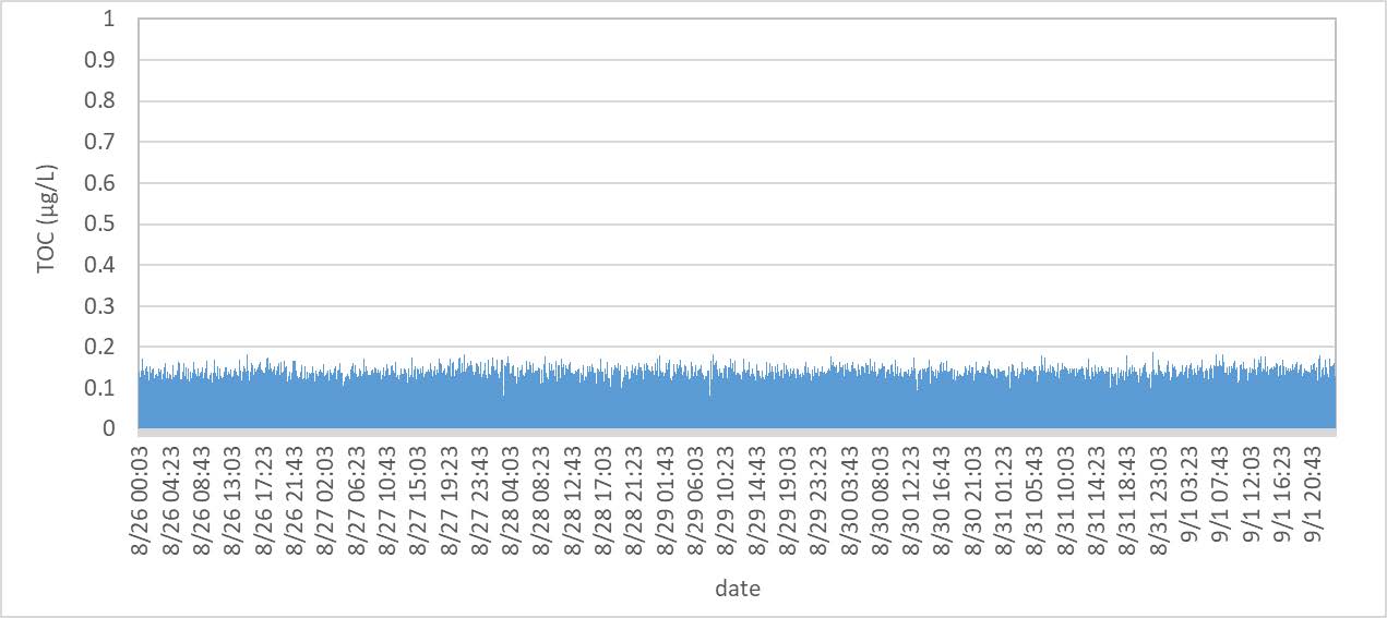
Lena knows that her fab already monitors the water, but the existing online TOC analyzer was installed in a different technology era. It is not optimized for the very low organic levels and the particularly persistent compounds that matter so decisively in today’s nanometer production. So her team decides to look more closely at one critical use point in the ultrapure water loop and installs a latest-generation online TOC analyzer designed specifically for ultrapure water monitoring in semiconductor manufacturing: Shimadzu’s new TOC‑1000e S (Figure 1).
The instrument itself is inconspicuous, about the size of a small desktop printer and light enough to be carried to different measurement points or mounted on the wall next to the water line. What interests Lena is the view it gives into the water’s “inner life” On the bright touchscreen, she sees a live TOC trend, updating every few minutes. Because the sample flows continuously through a short measurement line, the analyzer reacts quickly when the organic load changes. Small spikes now appear where the old TOC system showed only a flat line.
Over several weeks, Lena and her colleagues overlay these TOC curves with tool logs and maintenance records. They notice that organic peaks always follow certain process sequences and are strongest at one branch of the distribution system.
The analyzer cannot say which molecule is present, and it does not remove contamination. It does, however, tell the team when the water quality changes and where in the system this change first becomes visible.
With that information, the fab can work systematically instead of guessing. Engineers focus their inspections on a limited section of piping, adjust resin replacement intervals and tighten rinsing recipes around sensitive lithography steps. As these measures take effect, the TOC excursions at the use point become smaller and less frequent (Diagram 1). On Lena’s wafer maps, the once persistent defect pattern gradually fades into the background noise of everyday production.
Day‑to‑day operation benefits from practical advantages as well. Annual routine maintenance on the TOC-1000e S is simple and consists of replacing the excimer lamp and the pump head. All of these parts are accessible from the front of the device and require no tools. For calibration and validation, a compact vial sampler and certified standard solutions can be connected directly at the measurement point. And because the instrument can share its data as files, analog signals, or via a simple web browser on the factory network, engineers do not have to suit up and walk to the line every time they want to check what the hungry water is doing.
From clean water to everyday electronics
Lena has not “solved” the grand challenge of contamination in semiconductor fabs. No single tool can do that. But in her corner of the factory, one concrete and critical goal has been achieved. A stubborn defect pattern has been traced to its source and brought under control, and the process ramp now moves a step closer to the high yields the fab needs. Every avoided defect means fewer wafers scrapped, less energy and water wasted, lower costs incurred and more reliable chips reaching customers.
Those chips will quietly power everyday life: in smartphones and laptops, in cars and trains, in medical devices and communication networks. As future technology nodes shrink further to sub‑3 nm, the water that rinses each layer will only become more critical. Giving that “hungry water” a clear, quantitative voice through state-of-the-art TOC monitoring helps fabs manage invisible risks today and lays the foundation for the electronics that will shape tomorrow.